- What is a semiconductor?
- Chip, die, and integrated circuit
- What is a wafer?
- What is a fab?
- What is fabless?
- What is a foundry?
- What is an IDM?
- What is a node?
- What is yield?
- What is semiconductor IP?
- What is EDA?
- Photolithography and lithography
- Mask and reticle
- What is photoresist?
- What is etching?
- What is deposition?
- What is ion implantation?
- What is CMP?
- Metrology and inspection
- What is a cleanroom?
- What is cleanroom class?
- What is contamination?
- What is an air shower?
- What is gowning?
- HEPA and ULPA filters
- What is laminar flow?
- What is ESD?
- Front-end and back-end in chip manufacturing
- What is packaging?
- What is testing?
- What is reliability?
- Why are cleanrooms important in chip manufacturing?
- Other important terms in semiconductor cleanrooms
- The relationship between manufacturing terms and cleanroom terms
- Why semiconductor terminology matters for Vietnamese businesses
- Conclusion
The semiconductor industry is one of the most complex industries in the world. A chip as small as a fingernail can contain billions of transistors and is manufactured through hundreds to thousands of processing steps in an almost perfectly clean environment. Behind familiar products such as smartphones, computers, electric vehicles, AI devices, data centers, and defense systems lies a sophisticated technology chain that includes chip design, wafer manufacturing, photolithography, plasma etching, material deposition, metrology, packaging, and cleanroom control.
To understand the semiconductor industry, one must first understand its language. Terms such as fabless, foundry, wafer, yield, node, semiconductor IP, photolithography, cleanroom, contamination, photoresist, EUV, DUV, etching, deposition, CMP, and metrology are not merely technical vocabulary. They reflect how the industry operates, how value is created, and why chip manufacturing is so expensive, difficult, and strategically important.
This article explains the key terms in semiconductor manufacturing and chip cleanrooms in a clear and systematic way. It is suitable for beginners, managers, engineers from other fields, technical students, and businesses interested in the semiconductor supply chain.
What is a semiconductor?
A semiconductor is a class of materials whose electrical conductivity lies between that of a conductor and an insulator. The most important semiconductor material in today’s chip industry is silicon. Thanks to its ability to control electric current with high precision, silicon is used to manufacture transistors, diodes, sensors, memory, and many other electronic components.
In a modern chip, transistors act as tiny switches. When billions of these switches are arranged and connected according to a specific logic design, they form central processing units, graphics chips, AI chips, memory, power management chips, image sensors, or communication chips.
The semiconductor industry is not only about “making chips.” It is a broad ecosystem that includes chip design, wafer manufacturing, production equipment, materials, chemicals, design software, packaging, testing, distribution, and end applications.
Chip, die, and integrated circuit
A chip is the common term for an integrated circuit. An integrated circuit, abbreviated as IC, is a collection of tiny electronic components fabricated on the same semiconductor substrate.
Before becoming a finished chip, each circuit unit on a wafer is called a die. A single wafer can contain hundreds or thousands of dies. After production is completed, the wafer is cut into individual dies. Qualified dies are then packaged, tested, and integrated into final products.
In simple terms, the wafer is the large substrate, the die is each individual chip piece on the wafer, and the chip is the packaged die ready for use in electronic devices.
What is a wafer?
A wafer is a thin, round silicon disk with an extremely flat and clean surface, used as the substrate for chip fabrication. Instead of manufacturing chips one by one, semiconductor factories process an entire wafer at each production step. A wafer may contain many identical or different dies, depending on the product design.
Wafers commonly have diameters of 150 mm, 200 mm, or 300 mm. In modern chip fabrication plants, 300 mm wafers are widely used because their larger surface area allows more dies to be produced on a single substrate, thereby optimizing cost.
The wafer is the physical starting point of chip manufacturing. A wafer must go through many steps such as cleaning, oxidation, photoresist coating, photolithography, etching, deposition, ion implantation, polishing, metrology, and finally dicing. Even a tiny defect on the wafer can damage part or all of a die.
What is a fab?
Fab is short for fabrication plant, meaning a semiconductor manufacturing facility. This is where wafers are processed to create transistors, interconnect layers, insulating layers, and other microscopic structures on chips.
A fab is very different from an ordinary factory. It is a high-tech facility equipped with cleanrooms, machines worth millions to hundreds of millions of dollars, ultra-clean gas systems, ultra-pure water, high-purity chemicals, vibration control, temperature control, humidity control, and air pressure management.
An advanced fab may require tens of billions of dollars in investment. Much of the cost comes from photolithography tools, plasma etching equipment, thin-film deposition systems, metrology tools, automation systems, and cleanroom infrastructure.
In the industry, when people say “a company has a fab,” it means that the company has wafer manufacturing capability. When they say “fabless,” it means the company does not own a fab.
What is fabless?
Fabless refers to a business model in which a company designs chips but does not own a chip manufacturing plant. Fabless companies focus on architecture research, logic design, physical design, performance optimization, power consumption, software, ecosystem development, and commercialization.
After completing the design, a fabless company sends the design to a foundry for manufacturing. This model allows companies to avoid investing tens of billions of dollars in manufacturing facilities while focusing their resources on design capability and market development.
Well-known fabless companies include NVIDIA, AMD, Qualcomm, MediaTek, and Broadcom. These companies play major roles in processor chips, AI chips, communication chips, and mobile chips, even though most of their products are manufactured by external foundries.
Fabless is an important model because it opens the door for many companies to participate in the semiconductor industry without having to build a fab. As a result, the semiconductor value chain has become more specialized.
What is a foundry?
A foundry is a company that manufactures chips on behalf of chip design customers. If fabless companies are the designers, foundries are the ones that turn those designs into physical products on wafers.
A foundry must master process technology, operate fabs, control quality, optimize yield, protect customers’ design data, and support large-scale production. This is one of the highest-barrier segments in the semiconductor industry.
Large foundries usually offer multiple process nodes, ranging from mature nodes such as 180 nm, 90 nm, 65 nm, 40 nm, and 28 nm to advanced nodes such as 7 nm, 5 nm, 3 nm, or smaller. Customers choose a node depending on performance requirements, cost, power consumption, and product complexity.
Foundries are strategic links in the supply chain because most advanced chips in the world rely on the manufacturing capabilities of only a small number of leading manufacturers.
What is an IDM?
IDM stands for Integrated Device Manufacturer, meaning a company that both designs and manufactures chips. Unlike a fabless company, an IDM owns fabrication plants and manufactures many of its own products.
The IDM model used to be the dominant model in the semiconductor industry. Some IDM companies can design, fabricate, test, and sell chips under their own brands. The advantage of this model is tight control from design to manufacturing. The disadvantage is the enormous capital cost and the pressure to maintain advanced manufacturing technology.
IDMs are often common in segments such as memory, industrial chips, automotive chips, power chips, sensors, and certain microprocessor product lines.
The three main models can be summarized as follows: fabless companies design but do not manufacture; foundries manufacture for others; and IDMs both design and manufacture.
What is a node?
A node, or process node, refers to a generation of chip manufacturing technology. Terms such as 28 nm, 14 nm, 7 nm, 5 nm, and 3 nm are commonly used to refer to nodes.
In the past, the node number was fairly directly related to the physical size of certain transistor structures. However, in the modern semiconductor industry, these numbers are more like technology names, reflecting a combination of transistor density, performance, power consumption, transistor structure, and process capability.
More advanced nodes generally allow more transistors to be integrated into the same area, improving performance or reducing power consumption. However, advanced nodes also come with higher design costs, more complex manufacturing processes, more expensive equipment, and more difficult yield requirements.
Not every product needs the most advanced node. Automotive chips, industrial chips, power chips, sensors, microcontrollers, and many IoT chips still use mature nodes because they offer reasonable cost, high stability, and long product life cycles.
What is yield?
Yield is the percentage of dies or chips that meet quality requirements after manufacturing. It is a critical metric in semiconductor production.
For example, if a wafer contains 1,000 dies and 900 of them pass testing, the yield is 90%. If only 500 pass, the yield is 50%. The higher the yield, the lower the cost per good chip. Low yield can make a product unprofitable, even if the design is excellent.
Yield is affected by wafer quality, cleanroom cleanliness, equipment stability, the number of processing layers, die size, design complexity, node maturity, and defect control capability.
For large chips such as GPUs or AI chips, yield is especially important because the larger the die, the higher the probability of encountering a defect. A tiny dust particle, a lithography misalignment, or a material defect can ruin an entire die.
What is semiconductor IP?
Semiconductor IP refers to circuit design blocks that have already been developed, verified, and licensed for integration into chips. IP stands for intellectual property.
In modern chip design, no company wants to design everything from scratch if reliable IP blocks are already available. A chip may integrate many IP blocks such as CPU cores, GPU cores, memory controllers, PCIe, USB, HDMI, Ethernet interfaces, video encoders, digital signal processors, security blocks, or AI accelerators.
Using IP helps shorten design time, reduce technical risk, and improve reliability. However, companies must pay licensing fees and become partly dependent on IP providers.
In the semiconductor ecosystem, IP companies play a foundational role because they provide the “building blocks” for many different chip products.
What is EDA?
EDA stands for Electronic Design Automation. It refers to software tools used to design, simulate, verify, and optimize chips before manufacturing.
Designing a modern chip manually is impossible. Engineers need EDA software to describe logic, synthesize circuits, place transistors, route interconnects, check timing, verify power consumption, detect physical design errors, and validate the design.
EDA is the bridge between a design idea and the data that can be sent to a foundry. Without EDA, the modern chip industry would be almost impossible to operate.
Photolithography and lithography
Photolithography is the process of using light to transfer circuit patterns onto the surface of a wafer. It is a core step in chip manufacturing and determines the ability to create extremely small structures.
The basic process involves coating the wafer with a light-sensitive material called photoresist, exposing it to light through a mask or optical system to form a pattern, then developing the image and processing the material according to that pattern.
Photolithography can be compared to printing an ultra-small circuit drawing onto a wafer. However, unlike ordinary printing, the features on a chip may be only a few nanometers in size, requiring extremely high precision.
Common lithography technologies include DUV and EUV. DUV uses deep ultraviolet light, while EUV uses much shorter-wavelength extreme ultraviolet light, enabling smaller structures for advanced nodes.
Mask and reticle
A mask or reticle is a plate containing the design pattern used in the lithography process. Light passes through or reflects from the reticle to transfer the circuit image onto the wafer.
Each layer in a chip usually requires its own mask. A modern chip may require dozens to more than one hundred processing layers, meaning many different masks are needed. A mask set for an advanced node can be extremely expensive, sometimes costing millions of dollars or more.
Masks require extremely high precision. If a mask has a defect, that defect can be repeated across many wafers, causing significant losses. Therefore, mask inspection and protection are very important parts of semiconductor manufacturing.
What is photoresist?
Photoresist is a light-sensitive material coated onto the wafer before the lithography step. When exposed to light, the chemical properties of the photoresist change, allowing certain areas to be dissolved or retained after development.
Photoresist acts like a “light-sensitive ink” that helps form patterns on the wafer. After the photoresist pattern is created, steps such as etching or ion implantation process the wafer according to the opened or protected areas.
The quality of photoresist directly affects pattern sharpness, uniformity, and the ability to form small structures. For EUV, photoresist is one of the most technically challenging elements because it must be sensitive to light while maintaining high resolution and reducing noise.
What is etching?
Etching is the process of removing material from the wafer according to the pattern created by lithography. There are two main types: wet etching and dry etching.
Wet etching uses chemical solutions to dissolve material. Dry etching typically uses plasma or ions to remove material with higher precision. In modern chip manufacturing, dry etching is very important because it can create vertical, small, and precise structures.
Etching is like “carving” at the nanoscale. After photoresist defines the areas to keep and the areas to remove, etching removes material according to that pattern.
Errors in etching can change the dimensions of transistors, interconnects, or insulating layers, affecting chip performance and reliability.
What is deposition?
Deposition is the process of depositing material onto the wafer surface to create thin films. These layers may be metals, insulators, semiconductors, or other special materials.
A chip is not made only of silicon. It consists of many layers of materials stacked on top of one another, each with a specific function. Deposition builds these layers with thickness controlled at the nanometer or even angstrom scale.
Common deposition methods include CVD, or chemical vapor deposition; PVD, or physical vapor deposition; and ALD, or atomic layer deposition. ALD is especially important when extremely thin and uniform layers are needed on complex structures.
If lithography is the process of forming a pattern, and etching is the process of removing material, then deposition is the process of “adding material layers” onto the wafer.
What is ion implantation?
Ion implantation is the process of introducing dopant atoms into silicon to change the electrical properties of the material. It is an important step in creating n-type and p-type conductive regions in transistors.
The essence of semiconductors lies in the ability to adjust electrical conductivity through doping. Ion implantation allows precise control over dopant type, concentration, and depth in silicon.
After ion implantation, the wafer is usually heat-treated to activate the dopants and repair damage to the crystal lattice. If ion implantation is not accurate, transistors may malfunction, leak current, or fail to meet performance requirements.
What is CMP?
CMP stands for Chemical Mechanical Planarization or Chemical Mechanical Polishing.
During chip manufacturing, many layers of material are repeatedly deposited and etched, which can make the wafer surface uneven. CMP uses a combination of chemicals and mechanical force to flatten the surface and prepare it for subsequent processing steps.
Wafer flatness is extremely important because lithography requires a stable surface to print patterns accurately. If the surface is not flat, lithographic images can become distorted, reducing yield.
CMP is a quiet but crucial step. It is like leveling the foundation before continuing to build the next floors of an extremely tiny building.
Metrology and inspection
Metrology refers to measurement in semiconductor manufacturing. Inspection refers to defect detection. These two activities help a fab determine whether wafers are being processed correctly.
Metrology can measure material thickness, line width, alignment error, structural shape, material composition, and many other parameters. Inspection looks for defects such as particles, scratches, pattern defects, contamination, or process deviations.
In a fab, it is not possible to wait until the end of the process to inspect everything. If defects are discovered too late, many wafers may already have been ruined, causing major losses. Therefore, measurement and inspection are performed at many intermediate steps to control the process in real time.
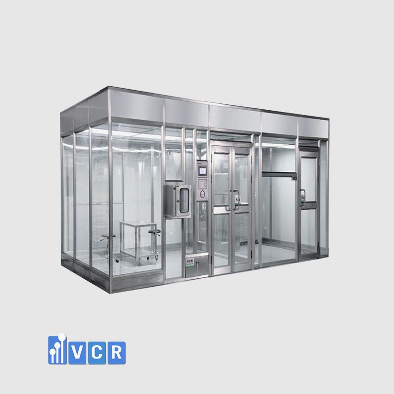
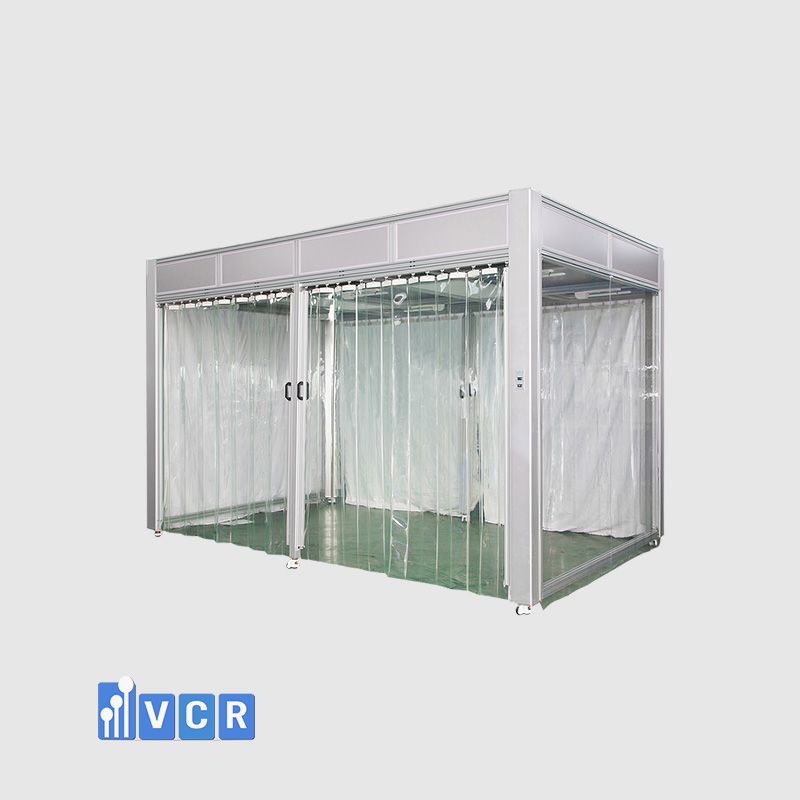
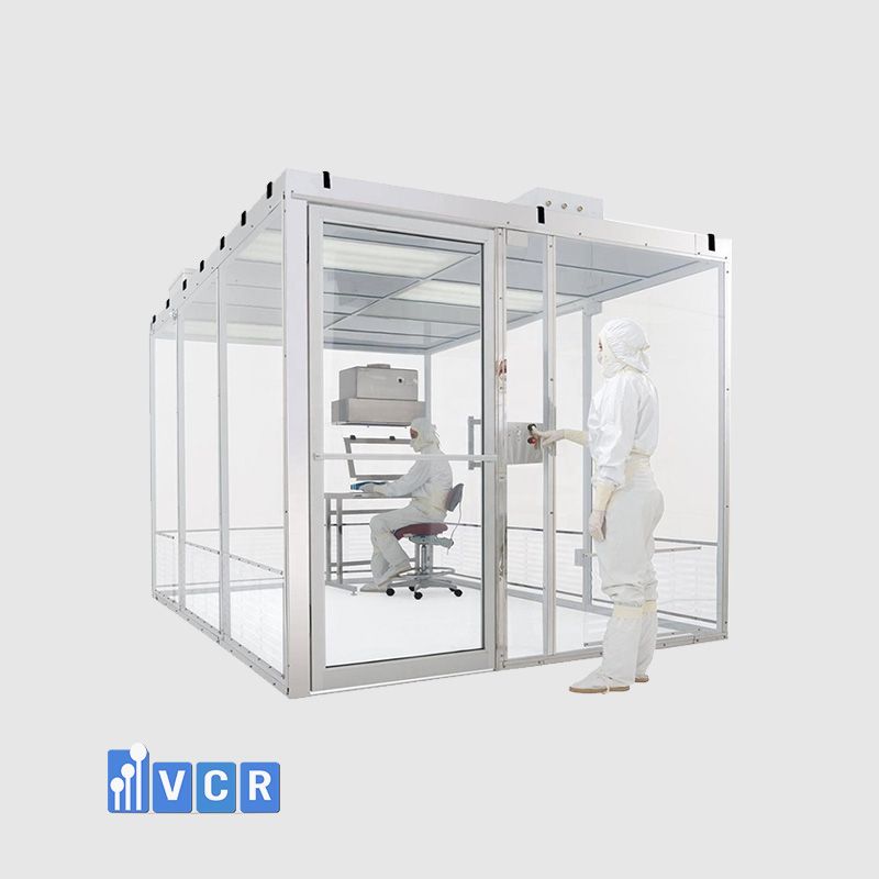
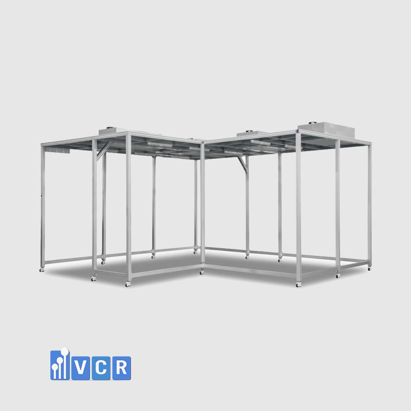
What is a cleanroom?
A cleanroom is an environment where particle count, temperature, humidity, pressure, airflow, and contamination levels are strictly controlled. In chip manufacturing, cleanrooms are mandatory.
A dust particle too small to be seen by the naked eye may still be many times larger than the features on a chip. If such a particle lands on a critical location on a wafer, it can break a circuit, cause a short circuit, or make a transistor fail.
Semiconductor cleanrooms use high-efficiency air filtration systems, controlled airflow, positive pressure, raised floors, filtered ceilings, special garments, and strict entry procedures.
The goal of a cleanroom is not simply to be “as clean as a hospital room,” but to achieve nanoscale industrial cleanliness, where dust, molecules, metals, ions, chemical vapors, and static electricity must all be controlled.
What is cleanroom class?
Cleanroom class refers to the cleanliness level of a cleanroom, usually classified by the number of particles in a given volume of air. A commonly used standard today is ISO 14644, with classes such as ISO Class 1, ISO Class 2, ISO Class 3, ISO Class 4, ISO Class 5, and higher.
The smaller the class number, the cleaner the room. In advanced semiconductor manufacturing, some areas require extremely clean environments, especially lithography zones, open-wafer processing areas, or surface inspection areas. Supporting areas may use lower cleanliness classes.
Not every part of a factory needs the same cleanliness level. Fabs are usually divided into multiple zones according to process requirements. This helps optimize cost because building and operating high-class cleanrooms is very expensive.
What is contamination?
Contamination refers to unwanted impurities. In chip manufacturing, contamination may come from particles, metals, organic molecules, ions, chemical vapors, water, gases, people, equipment, or consumable materials.
There are many types of contamination. Particle contamination refers to particulate contamination. Metal contamination refers to metallic impurities. Molecular contamination refers to molecular impurities. Organic contamination refers to organic residues. Ionic contamination refers to ionic impurities.
Each type of contamination can cause different defects. Particles can break or short circuits. Foreign metals can change electrical properties. Organic molecules can affect adhesion or chemical reactions. Unwanted chemical vapors can damage photoresist.
Contamination control is central to cleanroom management. A good fab does not only have advanced equipment; it must also have a highly disciplined contamination control system.
What is an air shower?
An air shower is an air-blowing chamber used before personnel enter a cleanroom. When a person wearing cleanroom garments steps into the air shower, high-speed air jets blow across the body to remove particles attached to the surface of the garments.
An air shower does not replace the entire cleanliness control process, but it is an important protective layer. It helps reduce the number of particles carried from outside areas into the cleanroom.
In a fab, people are one of the largest sources of particles. Skin, hair, fabric fibers, cosmetics, and body movement can all generate particles. Therefore, dressing procedures, movement, handling, and cleanroom entry are strictly controlled.
What is gowning?
Gowning is the process of putting on cleanroom garments. These garments usually include a coverall suit, hood, mask, goggles, gloves, boots, and accessories designed to prevent particle shedding and electrostatic discharge.
The goal of gowning is to prevent particles, hair, skin cells, and contaminants from people from spreading into the manufacturing environment. Cleanroom personnel must not only wear clean garments but also follow the correct dressing sequence, proper technique, and designated zones.
A small mistake in gowning can increase the risk of contamination. Therefore, many factories provide rigorous training on how to wear garments, move, hold tools, and work near wafers.
HEPA and ULPA filters
HEPA and ULPA are high-efficiency air filters used in cleanrooms.
HEPA filters can remove most very small airborne particles. ULPA filters offer even higher filtration efficiency and are used in environments that require stricter cleanliness. In semiconductor cleanrooms, air is usually filtered through ceiling-mounted filtration systems and then directed in a controlled flow toward the production area.
Filters are only one part of the system. For a cleanroom to operate effectively, it must combine airflow design, pressure control, construction materials, cleaning procedures, personnel access control, and continuous monitoring.
What is laminar flow?
Laminar flow is a smooth, stable airflow pattern with minimal turbulence, helping carry particles away from critical areas.
In semiconductor cleanrooms, airflow often moves from the ceiling down to the floor, through filters and return air systems. The goal is to prevent particles from remaining suspended or returning to the wafer surface.
If airflow is disturbed by improperly placed equipment, incorrect personnel movement, or poor room design, particles may accumulate in sensitive areas. Therefore, aerodynamic design in cleanrooms is very important.
What is ESD?
ESD stands for Electrostatic Discharge. In the semiconductor industry, ESD is a major risk because a small electrical pulse can destroy a component or reduce chip reliability.
People can accumulate static electricity when moving, touching materials, or wearing unsuitable clothing. When this charge discharges through a sensitive component, it may cause immediate damage or latent damage.
Cleanrooms and chip manufacturing areas commonly use anti-static flooring, grounding straps, suitable gloves, ESD packaging, ESD workbenches, and charge-control procedures.
ESD is especially important in die handling, packaging, testing, and component assembly.
Front-end and back-end in chip manufacturing
The semiconductor industry often divides the manufacturing process into front-end and back-end.
Front-end refers to the fabrication of semiconductor structures on the wafer, including transistors, insulating layers, metal layers, and interconnects inside the chip. This takes place in the fab and requires extremely clean environments.
Back-end can have two meanings depending on context. In chip design, back-end design refers to physical layout and routing. In manufacturing, back-end usually refers to the steps after wafer fabrication is complete, including die cutting, packaging, wire bonding, testing, sorting, and product finishing.
This distinction helps clarify the production chain: first, microscopic structures are created on the wafer; then the die is turned into a component that can be used in electronic systems.
What is packaging?
Packaging is the process of enclosing a chip. It protects the die, connects the die to the outside world, and allows the chip to be mounted on a circuit board.
Packaging is not simply “wrapping the chip.” The package affects electrical performance, heat dissipation, mechanical durability, product size, and system integration. For high-performance chips, packaging is increasingly becoming a strategic factor.
Advanced packaging technologies such as 2.5D, 3D, chiplet, interposer, fan-out, and hybrid bonding make it possible to combine multiple dies in one package, increasing bandwidth, reducing latency, and improving system performance.
In the AI era, advanced packaging is becoming increasingly important because not all improvements come from smaller nodes. The way multiple chips are connected also creates major advantages.
What is testing?
Testing is the process of checking whether a chip operates correctly. Testing can take place at the wafer level before dicing, known as wafer probing, and after packaging, known as final test.
Testing helps classify good chips, defective chips, or chips that operate at different performance levels. In some cases, chips with the same design may be sorted into different product lines based on test results.
Semiconductor testing does not only confirm whether a chip turns on. It also measures performance, power consumption, thermal stability, speed, memory errors, signal characteristics, and operation under different conditions.
What is reliability?
Reliability refers to the ability of a chip to operate dependably over time. A chip must not only pass initial testing but also function stably for many years under different temperature, voltage, and workload conditions.
Reliability tests may include high-temperature testing, humidity testing, thermal shock, electrical aging, high-voltage testing, and power cycling. Requirements are especially strict for automotive, aerospace, industrial, and medical chips.
A chip failure in a smartphone may be inconvenient. But a chip failure in a car, medical device, or industrial control system can have serious consequences. Therefore, reliability must not be overlooked.
Why are cleanrooms important in chip manufacturing?
Cleanrooms are the foundation of chip manufacturing because the structures on chips are extremely small. In the ordinary world, dust is almost unavoidable. But inside a fab, a dust particle can be like a “giant boulder” compared with a transistor.
Without cleanroom control, yield decreases, costs increase, product defects rise, and the process becomes unstable. Cleanrooms do not only reduce dust; they control the entire production environment, including air, water, gases, chemicals, materials, people, equipment, and procedures.
An advanced fab is essentially a combination of nanotechnology, chemistry, physics, precision mechanics, automation, data, quality management, and disciplined operations. Within it, the cleanroom is the central space that protects wafers from the outside world.
Other important terms in semiconductor cleanrooms
AMC, or airborne molecular contamination, refers to molecular contamination in the air. This type of contamination is difficult to control because it is not always visible like particles.
UPW, or ultra-pure water, is extremely purified water used to rinse wafers. Water in a fab must be much cleaner than ordinary drinking water because ions, microorganisms, particles, or metals can all cause defects.
Process gases include nitrogen, argon, oxygen, hydrogen, and special gases used in deposition, etching, cleaning, and surface treatment.
FOUP, or front opening unified pod, is a specialized container used to transport wafers inside a fab. FOUPs protect wafers from contamination and are often integrated with automated transport systems.
AMHS, or automated material handling system, is the automated system used to move materials inside a fab. In modern factories, wafers are transported by overhead automated systems instead of relying heavily on people.
A mini-environment is a localized clean environment inside equipment or wafer storage areas, helping protect wafers better even when the surrounding room has a lower cleanliness class.
The relationship between manufacturing terms and cleanroom terms
Semiconductor terms do not exist separately. They are connected into a unified manufacturing chain.
A fabless company designs a chip using EDA tools and multiple semiconductor IP blocks. The design is sent to a foundry. The foundry manufactures the chip in a fab on silicon wafers. The fab uses a specific process node. During production, wafers go through photolithography, photoresist coating, etching, deposition, ion implantation, CMP, metrology, and inspection. All of this takes place in a cleanroom with contamination control, ESD control, airflow management, HEPA and ULPA filtration, gowning, and air showers. The wafer is then tested, diced into dies, packaged, final-tested, and shipped.
If one link is weak, the entire chain can be affected. A good design with low yield increases cost. An advanced node with unstable cleanroom conditions creates many defects. Modern equipment without contamination control cannot ensure product quality. Good packaging without strict testing increases quality risk.
Therefore, chip manufacturing requires overall precision, not just excellence in a single process step.
Why semiconductor terminology matters for Vietnamese businesses
Vietnam is paying increasing attention to the semiconductor industry, from chip design, testing, and packaging to workforce development and participation in the global supply chain. To participate effectively, businesses and workers need to understand fundamental terminology correctly.
Understanding “fabless” shows that opportunities do not necessarily begin with building a fab. Understanding “foundry” highlights the enormous barriers in wafer manufacturing. Understanding “wafer” and “yield” reveals the economic nature of chip production. Understanding “node” helps avoid the misconception that smaller is always better for every application. Understanding “cleanroom” shows that semiconductor manufacturing is a game of operational discipline, environmental control, and extremely high quality standards.
For Vietnam, practical opportunities may lie in IC design, supporting EDA software, testing, packaging, auxiliary materials, supporting equipment, workforce training, factory automation, and technical services for the semiconductor supply chain.
Conclusion
Semiconductor manufacturing is a combination of materials science, physics, chemistry, precision mechanics, automation, information technology, and quality management. Terms such as fabless, foundry, wafer, yield, node, semiconductor IP, photolithography, etching, deposition, CMP, metrology, cleanroom, contamination, HEPA, ULPA, ESD, packaging, and testing are key to understanding how a chip is made.
From the outside, a chip may look like a small electronic component. But inside, it is the result of thousands of design decisions, hundreds of manufacturing steps, a strictly controlled cleanroom environment, and a global supply chain of extremely high precision.
In the era of AI, electric vehicles, automation, high-tech defense, and digital transformation, semiconductor knowledge is no longer reserved only for chip engineers. It is a foundation that helps businesses, managers, and technology learners recognize their opportunities, risks, and position in one of the most important industries of the 21st century.